
After many days of work and
research I am now ready with Microchip PICKit2 programmer clone with Minimum
and easily available parts with almost full functionality necessary for
programming. This is based on the microchip PICKit2. Unlike the original, it also support
ICSP (In Circuit Serial Programming) as well as provision of 8/14/18/20/28/40
pin programming adaptor is also incorporated to make programming easier. It supports 5V as well as 3.3V devices. The
controller is fully compatible with the MICROCHIP PICKit2 v2.61 /Microchip MPLAB
IDE and as the firmware is
developed by Microchip all devices are supported by this
programmer like : PIC10F (DIP8) PIC12F (DIP8) PIC16F (DIP14, 18, 20,
28 and 40) PIC18F (DIP18, 20, 28 and 40) dsPIC30F (DIP28 and 40). I
personally program and verify 16F628A without any problem , in theory, they require Vpp before
Vdd, but actually, it works anyway !. I try my best to reduce the component count
as low as possible without losing functionality, also I keep in mind that some
of the components used in Microchip original design is not easily available everywhere
therefore the components I used here, except
18F2550 is of general purpose type.
Inductor L1 is not so critical you can use any value between 450uH-1mH but the
current rating should be at least 10mA or more. You can arrange the inductor
from any 20/25W old CFL (generally 1mH inductor used in CFL’s).

The push button used here to force PIC18F2550 to enter in bootloader
mode at power-up, or trigger chip programming after power-up (Generally
used for standalone programming, and almost useless here and incorporated only as some conditions
demands sometimes).
Here for 3.3V devices the required VDD is generated using LM317 regulator because the USB supply varies from 4.75V to
5.25V from PC to PC


ICSP
MALE & FEMALE CONNECTOR
The "POWER"
LED will be constantly lit when PICkit2 is power up.
The "TARGET" LED
will lit when PICKit2 supply Vdd to external circuits.
(you can even omit this if you like)
The "BUSY" LED will lit when PICkit2 is communicating with PC or
programming a chip.
Resistors
R9, R14, and R19 are used to limit the current to LEDs.
Two pins (i.e. D+ and D-) of PIC18F2550 are
used to connect to USB Data+ and Data- to PC and used for communication.
An internal 3.3V regulator is used to power the internal transceiver. A 0.47uF capacitor C2 (use only 0.47uF polyester
type capacitor here) is used to
stabilize the 3.3V supply.
PICkit 2 is a USB powered, low-power device, it gets all the power from
PC USB +5V power supply. The USB port
provides a 5 V(±5%) supply and
maximum permissible load current is 100mA in USB 2.0. When the total
current for both target and the PICkit2 programmer exceeds this current limit,
the USB port may turn off. If this situation arises then target needs external
power supply.
Since PICKit2 itself can draw current as high as 75mA, therefore the target circuit should be limited to 25mA if PICkit2 programmer supplies power. It is always a good in practice to use external power supply when programming hi-performance chipsets, like dsPIC30Fs (they normally consume more current).
Since PICKit2 itself can draw current as high as 75mA, therefore the target circuit should be limited to 25mA if PICkit2 programmer supplies power. It is always a good in practice to use external power supply when programming hi-performance chipsets, like dsPIC30Fs (they normally consume more current).
Pin details of some male and female USB connectors given below for your
convenience.

Important Note :-During the construction of this programmer I face a strange problem
related to the USB, my PC is not detecting the hardware, then I searched
datasheets and web for solution but nothing found , after that I connect a pull-up resistor (i.e.4.7k) from
pin No.14 (i.e. VUSB) to +5V supply(i.e. Vdd) ( as shown in figure below) …..and
it works perfectly as a HID device…..in
case, if you also face the similar situation then try this, otherwise go for
straight way.


Boost voltage Generation and Control
VPP Boost voltage Generation and Control
As the VPP voltage requirement for PIC varies from 3.3V (dsPIC33F) to 13V (PIC18F ) and as USB port supplies only 5 volt. Therefore a switch mode boost circuit (as shown above) is used to generate the required target voltage ("VPP").
As the VPP voltage requirement for PIC varies from 3.3V (dsPIC33F) to 13V (PIC18F ) and as USB port supplies only 5 volt. Therefore a switch mode boost circuit (as shown above) is used to generate the required target voltage ("VPP").
To stabilize the power supply of the switch
mode boost circuit and damp the possible noise , C7 is used, and they should be
placed as close as possible to inductor L1. The PIC18F2550 controls the switching
of Q1 (i.e. BC548 or you can use any general purpose transistor
here) .The current handling capacity for inductor L1 should be at least
10mA. When Q1 is on, electric current flow through L1 and Q1, energy is stored
in L1. When Q1 is turned off, a high voltage is generated at collector of Q1.
The diode D1 i.e. IN4148 conducts and
charged the capacitor C1, electric current will keep flowing through L1
and D1. This will charge the capacitor and raise its voltage to desired VPP
voltage. Resistor R2 and R3 generate a feedback signal which is send back to
PIC18F2550 pin No.2. With this "VPP_FEEDBACK" signal, the PIC18F2550
precisely adjust the switching frequency
of Q1. Thus this feedback boost circuit can generate the required "VPP " voltage.
R4, R5, R6, Q2 and Q4 are used as ON/OFF
switch for VPP. When "VPP_ON" is set at high logic by PIC18F2550, Q2
will be on, which will then turn on Q4, and the voltage on C1 will appear on
ICSP VPP Pin No.1. When a low logic is send to Q2 by PIC18F2550, Q2 and Q4 will
be turned off. This in turn cut off the VPP supply to external circuit. When Q4
and Q3 are both off, the VPP Pin No.1 is in floating condition. The PIC18F2550
can turn on Q3 and it will clamp VPP Pin to ground. This has been used for PICkit2 self test procedure,. thus overall
VPP control procedure makes it possible to turn ON and turn OFF VPP at any time.
Note :- The voltage rating of capacitor C1
should be 25v or more . R2 and R3
should have 1% or better accuracy. If
possible try to use Schottky type diode(like
BAT54) in place of D1 to ensure
low voltage drop otherwise use
IN4148.
Important Note :-Generally PICkit2 can provide Vdd to power external circuit but in situations where target is powered by external source it is necessary to remove the “Vdd selection(3.3v-5v) jumper J1 to isolate the internally generated Vdd from the external Vdd, otherwise target device may be damaged.
Software, Firmware & Schematics
You can download the required software’s, firmware & Eagle schematics from the links given below, also it is recommended to read the “PICKIT 2 user manual” as well as “Programmer-To-Go_User_Guide” placed in help section of software before using this.
Firmware :- BOOTLOADER.HEX
Remember :- Remember
that, only BOOTLOADER.hex file need to be burned in the 18F2550 and nothing else. After that when you connect the PICKIT2 to PC
using PICKit2 v2.61 software it shows a message “ No OS found, download the required firmware”….then go to the TOOLS > Download pickit2 operating
system…. And you find that target folder contain the required firmware file PK2V023200.hex, choose it , wait for a minute
till the firmware is successfully uploaded to 18F2550 and enjoy!!!!!

One more thing you need a extra programmer to burn the BOOTLOADER.hex to the 18F2550, a serial
based JDM programmer is suitable for that. For your convenience JDM based programmer schematic
and required software link is provided below

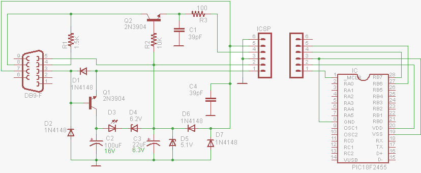
JDM
programmer schematic
Software
for JDM programmer :- WinPic800

Still if you have
any query or questions feel free to comment I will try my best…….
Regards
Rishi kumar Sumal


